Semiconductor Inspection Using SWIR Cameras
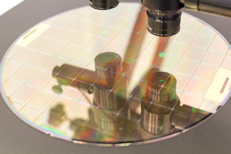
One of machine vision’s most important contributions to making affordable integrated circuits (ICs) and solar panels is the use of InGaAs SWIR cameras to inspect silicon devices by ‘seeing’ through the material. Silicon absorbs visible and infrared wavelengths, making it ideal for most imaging detectors. But silicon can’t be used for infrared detection because it loses sensitivity past 900 nm and is transparent to wavelengths longer than 1120 nm. This transparency to SWIR imaging enables SWIR applications like photoemission failure analysis of ICs, imaging of IC and MEMs layers for alignment errors, plus inspection of solar cells for cracks and defects. Even imaging through a solid ingot block of 4x4x10 inches is achieved by InGaAs SWIR cameras. This enables rejecting silicon ingots with voids or carbon deposits, BEFORE wasting time and materials cutting the ingot or boule into wafers. (Note that one face of the wafer or ingot needs to be polished to avoid scattering of the image and a long-pass filter used to avoid visible reflections.)
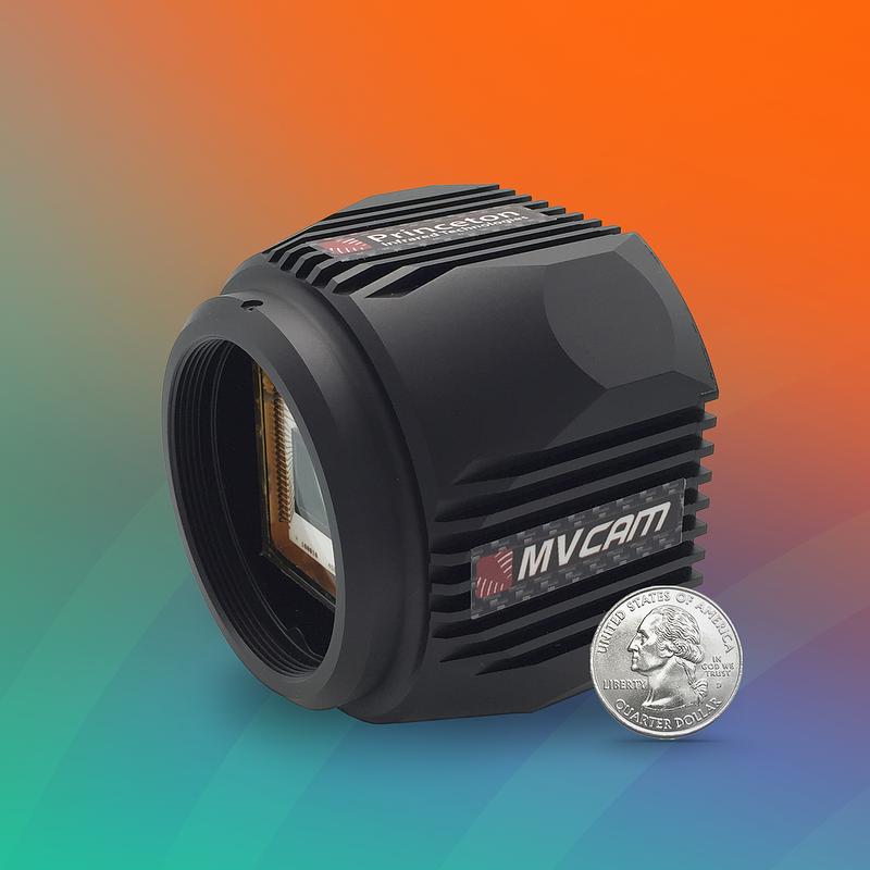
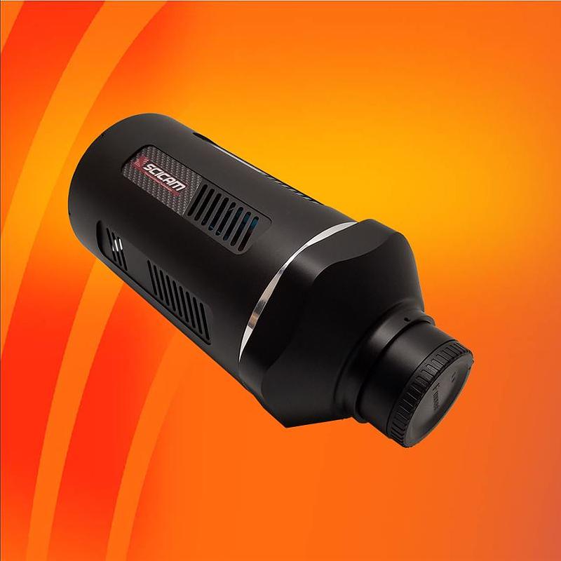
Selecting the best SWIR camera for a silicon semiconductor inspection application depends on the production process involved and the presentations available for the object to be inspected. When snapshot imaging is needed, 2-D SWIR cameras should be considered. Both PIRT 2-D SWIR cameras offer HD resolution (1024-pixel width) with 12-μm pixels, providing wide FOV and detailed resolving power. The PIRT MVCam SWIR camera is a compact temperature stabilized megapixel imager capable of keeping up with fast moving objects utilizing its 100 full frame per second acquisition rate and high sensitivity and runs up to 385 fps when windowed to a 512x512 image. The 1280SciCam scientific SWIR camera runs almost as fast but also can run the detector deeply cooled to enable 2 minutes integration times, ideal for imaging faint photoemission from shorted IC transistors encountered in IC Failure Analysis.

 MVCam
MVCam 1280SciCam